Part A. Physical Layer Specification
vAtlanta r00
This Part describes the Bluetooth Low Energy physical layer.
1. Scope
Bluetooth Low Energy (LE) devices operate in the unlicensed 2.4 GHz ISM (Industrial Scientific Medical) band. A frequency hopping transceiver is used to combat interference and fading.
Two modulation schemes are defined. The mandatory modulation scheme (“1 Msym/s modulation”) uses a shaped, binary FM to minimize transceiver complexity. The symbol rate is 1 Msym/s. An optional modulation scheme (“2 Msym/s modulation”) is similar but uses a symbol rate of 2 Msym/s.
The 1 Msym/s modulation supports two PHYs:
LE 1M, with uncoded data at 1 Mb/s;
LE Coded, with the Access Address, Coding Indicator, and TERM1 coded at 125 kb/s and the payload coded at either 125 kb/s or 500 kb/s.
A device shall support the LE 1M PHY. Support for the LE Coded PHY is optional.
The 2 Msym/s modulation supports two PHYs:
LE 2M, with uncoded data at 2 Mb/s with BT=0.5.
LE 2M 2BT, with uncoded data at 2 Mb/s with BT=2.0. This PHY may only be used with the Channel Sounding feature.
A device may optionally support Channel Sounding (CS). The modulation requirements for LE 1M, an optional LE 2M, and an optional LE 2M 2BT also apply to any CS_SYNC packet (see [Vol 6] Part H, Section 2). The CS tone transmitter and receiver requirements are specified in Section 3.4 and Section 6, respectively.
CS uses an additional modulation scheme known as amplitude-shift keying (ASK). When using ASK, symbols are sent by transmitting a fixed-amplitude carrier wave at a fixed frequency for a specific time duration.
A Time Division Duplex (TDD) scheme is used on all PHYs. The specification defines the requirements for a Bluetooth radio for the Low Energy radio.
Requirements are defined for two reasons:
Provide compatibility between radios used in the system
Define the quality of the system
An LE radio shall have a transmitter or a receiver, or both.
The LE radio shall fulfill the stated requirements for the operating conditions declared by the equipment manufacturer (see Section A.1).
The Bluetooth SIG maintains regulatory content associated with Bluetooth technology in the 2.4 GHz ISM band on its web site, at https://www.bluetooth.com/regulatory-requirements/.
2. Frequency bands and channel arrangement
The LE system operates in the 2.4 GHz ISM band at 2400 MHz to 2483.5 MHz. The LE system uses 40 RF channels with center frequencies at a 2 MHz spacing from 2402 MHz to 2480 MHz.
An LE system supporting CS uses 72 RF channels for CS exchanges. These RF channels have center frequencies at 2402 + k MHz, where k is an integer from 2 to 22 and 26 to 76.
3. Transmitter characteristics
The requirements stated in this section are given as power levels at the antenna connector of the LE device; this is also referred to as the radiative transmit power level of the device. If the device does not have a connector, a reference antenna with 0 dBi gain is assumed. Power level values used in HCI commands, HCI events, Advertising physical channel PDUs, and Link Layer Control PDUs shall be assumed to be the radiative transmit power level of the device unless specified otherwise.
Due to the difficulty in making accurate radiated measurements, systems with an integral antenna should provide a temporary antenna connector during LE PHY qualification testing.
For a transmitter, the radiative transmit power level at the maximum power setting shall be between 0.01 mW (-20 dBm) and 100 mW (+20 dBm).
Using high transmit power in use cases where short ranges could be encountered can cause the receiver on the remote device to be saturated and result in link failure. The LE Power Control Request feature can be used to adjust a connected remote device’s transmit power level based on the receiver’s signal level. When the LE Power Control Request feature is used on a connection with long connection intervals, devices should use reliable RSSI measurements from recent connection events to determine whether or not to send power control requests. When a device is capable of adjusting its transmit power level using the LE Power Control Request feature, the difference between any two adjacent transmit power levels supported by the radio design should be no greater than 8 dB. When the LE Power Control Request feature is not supported by either the local or remote device, implementers should avoid use of high output power in such scenarios or employ a mechanism for switching between two or more transmit power levels in an attempt to establish, re-establish, or maintain connections.
The output power control of a device may be changed locally, for example to optimize the power consumption or reduce interference to other equipment.
Bluetooth devices are classified into power classes based on the radiative transmit power level at the maximum power setting the LE PHY supports (Pmax), as defined in Table 3.1.
Power Class | Requirements |
|---|---|
1 | 100 mW (+20 dBm) ≥ Pmax > 10 mW (+10 dBm) |
1.5 | 10 mW (+10 dBm) ≥ Pmax > 2.5 mW (+4 dBm) |
2 | 2.5 mW (+4 dBm) ≥ Pmax > 1 mW (0 dBm) |
3 | 1 mW (0 dBm) ≥ Pmax ≥ 0.01 mW (-20 dBm) |
3.1. Modulation characteristics
The modulation is Gaussian Frequency Shift Keying (GFSK) with a bandwidth-bit period product BT=0.5. The modulation index shall be between 0.45 and 0.55. A binary one shall be represented by a positive frequency deviation, and a binary zero shall be represented by a negative frequency deviation.

For each transmission the minimum frequency deviation,
which corresponds to a 1010 sequence, shall be no smaller than ±80% of the frequency deviation with respect to the transmit frequency, which corresponds to a 00001111 sequence.
The minimum frequency deviation shall never be less than 185 kHz when transmitting at 1 megasymbol per second (Msym/s) symbol rate and never be less than 370 kHz when transmitting at 2 Msym/s symbol rate. The symbol timing accuracy shall be better than ±50 ppm.
The zero crossing error is the time difference between the ideal symbol period and the measured crossing time. This shall be less than ±18 of a symbol period.
See Figure 3.1 for the definitions of some symbols and terms in these requirements.
3.1.1. Stable modulation index
An LE device with a transmitter that has a stable modulation index may inform the receiving LE device of this fact through the feature support mechanism (see [Vol 6] Part B, Section 4.6). The modulation index for these transmitters shall be between 0.495 and 0.505. A device shall only state that it has a stable modulation index if that applies to all LE transmitter PHYs it supports.
A transmitter that does not have a stable modulation index is said to have a standard modulation index.
3.1.2. Modulation characteristics of Channel Sounding steps
During Channel Sounding steps where a CS_SYNC packet is present (see [Vol 6] Part H, Section 2) and the LE 2M 2BT PHY is used, the modulation characteristics are identical to those described in Section 3.1 with the following exceptions:
The 2 Msym/s transmission rate shall be used with a bandwidth-bit period product BT=2.0.
The minimum frequency deviation at the center of the symbol shall never be less than 420 kHz.
3.1.3. SNR control for Channel Sounding steps
An LE device may have a transmitter that is capable of adjusting its SNR output within a given range for modulated transmissions. There are five different SNR levels defined in Table 3.2, each identified by an SNR Output Index (SOI).
SNR Output Index (SOI) | SNR Output Level (dB) | Mandatory/Optional/Conditional |
|---|---|---|
0 | 18 | C.1 |
1 | 21 | C.1 |
2 | 24 | C.1 |
3 | 27 | C.1 |
4 | 30 | C.1 |
| ||
Let ˆx(k,t) be the continuous version of the observed CS_SYNC packet transmitted by the IUT at step k, as defined in [Vol 6] Part H, Section 3.1.1. Let ˆφ(k,t) be the phase of the observed ˆx(k,t).
Let φideal(k,t) represent the phase trajectory generated from the modulated bit sequence at step k, using the modulation rules described in Section 3.1.2.
Let SNRdesiredTX be the configured SNR value for the IUT.
Let T represent the integration period for the entire CS_SYNC packet transmitted at step k.
Let τ0, f0, and φ0 represent the best fit timing, frequency, and phase alignment respectively between the observed signal transmitted by the IUT and φideal(k,t).
The IUT transmitter SNR is then computed using equation:
The SNR control error can be computed:
The SNR control error shall satisfy:
and the standard deviation of the randomness of the added error shall satisfy:
for 95% of the steps.
3.2. Spurious emissions
3.2.1. Modulation spectrum
For products that transmit modulated packets and also follow the requirements of FCC part 15.247, the minimum 6 dB bandwidth of the transmitter spectrum shall be at least 500 kHz using a resolution bandwidth of 100 kHz.
3.2.2. In-band spurious emission
An adjacent channel power is specified for channels at least 2 MHz from the carrier when transmitting with1 Msym/s modulation (applies to the LE 1M and LE Coded PHYs) or at least 4 MHz from the carrier when transmitting with 2 Msym/s modulation (applies to the LE 2M and LE 2M 2BT PHYs). This adjacent channel power is defined as the sum of the measured power in a 1 MHz bandwidth.
The spectrum measurement shall be performed with a 100 kHz resolution bandwidth and an average detector. The device shall transmit on an RF channel with the center frequency M and the adjacent channel power shall be measured on a 1 MHz RF frequency N. The transmitter shall transmit a pseudo random data pattern in the payload throughout the test.
Frequency offset | Spurious Power |
|---|---|
2 MHz (|M-N| = 2) | -20 dBm |
3 MHz or greater (|M-N| ≥ 3) | -30 dBm |
Frequency offset | Spurious Power |
|---|---|
4 MHz (|M-N| = 4) | -20 dBm |
5 MHz (|M-N| = 5) | -20 dBm |
6 MHz or greater (|M-N| ≥ 6) | -30 dBm |
Exceptions are allowed in up to three bands of 1 MHz width, centered on a frequency which is an integer multiple of 1 MHz. These exceptions shall have an absolute value of -20 dBm or less.
3.2.3. Out-of-band spurious emission
The equipment manufacturer is responsible for the ISM out-of-band spurious emissions requirements in the intended countries of sale.
3.3. Radio frequency tolerance
The deviation of the center frequency during the packet shall not exceed ±150 kHz, including both the initial frequency offset and drift. The frequency drift during any packet shall be less than 50 kHz. The drift rate shall be less than 400 Hz/µs.
The limits on the transmitter center frequency drift within a packet is shown in Table 3.5.
Parameter | Frequency Drift | ||||||||||||||||||||||||||||||||||||||||||||||||
|---|---|---|---|---|---|---|---|---|---|---|---|---|---|---|---|---|---|---|---|---|---|---|---|---|---|---|---|---|---|---|---|---|---|---|---|---|---|---|---|---|---|---|---|---|---|---|---|---|---|
Maximum drift | ±50 kHz | ||||||||||||||||||||||||||||||||||||||||||||||||
Maximum drift rate1 | 400 Hz/μs | ||||||||||||||||||||||||||||||||||||||||||||||||
1The maximum drift rate is allowed anywhere in a packet. | |||||||||||||||||||||||||||||||||||||||||||||||||
3.4. Stable phase
Devices supporting the CS feature shall support the generation of an RF signal with a phase that is stable during the period of T_PM_MEAS. T_PM_MEAS shall be equal to the CS step mode-2 duration as defined in [Vol 6] Part H, Section 4.3.3 using the maximum values allowed for the following:
Phase measurement period
Antenna switch period
Ramp-down period
Interlude periods
Number of antenna paths
This requirement shall also be applicable to the CS tone duration defined for CS step mode-3 as described in [Vol 6] Part H, Section 4.3.4.
Let ϕ[n] be the unwrapped phase of the signal, where unwrap refers to the operation that corrects the radian phase of the array elements by adding multiples of ±2 pi when absolute jumps between consecutive array elements are larger than pi. Also, let ϕ[n] be sampled at a 1 µs interval during the period of T_PM_MEAS (in microseconds), where N is equal to (T_PM_MEAS in microseconds), and where n is an integer in the range of 1 to N.
Let Δϕ be the phase detrend factor for the absolute unwrapped phase signal, defined as:
So that the detrended phase is expressed as:
Let be the mean value of the detrended sequence, expressed as:
So, the final, zero-mean, detrended phase vector is given by:
Following these definitions, 95% of the absolute values of ϕzmd[n] shall be 20 degrees or less.
3.5. Frequency measurement and generation in Channel Sounding
The structure for CS subevents is defined in [Vol 6] Part H, Section 4.4. Each CS subevent contains K + M CS steps, k = 1, …, K + M. The first M steps within the subevent are CS mode-0 steps as defined in [Vol 6] Part H, Section 4.3.1, and are followed by K non-mode-0 steps. Each non-mode-0 step that has CS tones contains P phase measurement periods, where 1 ≤ P ≤ (N_AP plus any added CS tone extensions). N_AP is defined in Section 5.3 and CS tone extensions are defined in [Vol 6] Part H, Section 4.3.
Denote the expected start and end times of the CS tone transmitted by a device for the kth step in phase measurement period p, as and , respectively, if a transmitted CS tone exists within that step and phase measurement period. Within this phase measurement period, the time t = 0 corresponds to the start of the first scheduled transmission within a CS subevent.
Denote f0[k] as the nominal frequency of the CS Channel for step k as defined in Section 2.
Denote f[k, p] as the average frequency of the transmitted CS tone during the interval .
3.5.1. Fractional frequency offset
The fractional frequency offset (FFO) is the frequency offset normalized by the carrier frequency. The FFO for the kth mode-0 step within a subevent is denoted as FFO[k], and is given by
where FAE[k] is the value of the FFO actuation error (FAE) for the CS channel used in step k taken from the mode-0 FFO actuation error table of the local Controller. The FAE is communicated by the reflector and represents a known additional fractional frequency offset error on mode-0 channels.
The value of each FAE for each CS channel shall satisfy -4 ppm ≤ FAE ≤ 3.96875 ppm. For all CS mode-0 steps, the absolute value of FFO[k] shall be less than 50 ppm.
For all CS mode-0 steps within a subevent, the values of |FFO[k] − FFO[1]| shall be less than 1 ppm for 2 ≤ k ≤ M.
The receiving device of a mode-0 CS tone may estimate and report the FFO of the transmitting device of the mode-0 CS tone. In this case, the FFO is given by
where fRX[k] is the receiving device’s estimate of the average frequency of the received CS tone in step k. The receiving device should compensate for its own local frequency actuation error (LFAE) as defined in Section 6.3, as part of its FFORX[k] estimate. The term FFORX* is used to refer to the estimated FFO derived from all mode-0 CS tones within a CS subevent.
3.5.2. Expected transmitted frequencies
The FFO for a CS subevent, FFOE, is defined as the value of FFO[1] for the device transmitting the CS tone during the first mode-0 step of a subevent.
The expected transmit frequency of the CS device for the kth step is given by
where k = M + 1, …, K + M.
For the non-mode-0 steps M + 1 ≤ k ≤ M + K, and for each phase measurement period 1 ≤ p ≤ P[k], the average transmitted frequency f[k, p] shall satisfy
for 95% of CS tone transmissions within non-mode-0 steps.
The center frequency of the transmitted CS_SYNC packet within any non-mode-0 step shall not deviate by more than 20 kHz with respect to the expected transmit frequency fE[k], for 95% of CS_SYNC transmissions within non-mode-0 steps.
The center frequency of the transmitted CS_SYNC packet within any mode-0 step 1 ≤ k ≤ M shall not deviate by more than 20 kHz with respect to the average frequency of the transmitted CS tone f[k, 1], for 95% of CS_SYNC transmissions within mode-0 steps.
4. Receiver characteristics
The reference sensitivity level referred to in this section is -70 dBm. The packet error rate corresponding to the defined bit error ratio (BER) shall be used in all receiver characteristic measurements.
4.1. Actual sensitivity level
The actual sensitivity level is defined as the receiver input level for which the BER specified in Table 4.1 is achieved.
Maximum Supported Payload Length (bytes) | BER (%) |
|---|---|
1 to 37 | 0.1 |
38 to 63 | 0.064 |
64 to 127 | 0.034 |
128 to 255 | 0.017 |
The actual sensitivity level of the receiver for a given PHY shall be as specified in Table 4.2. This shall apply when receiving signals specified in Section 3 together with any combination of the following allowed parameter variations:
Initial frequency offset
Frequency drift
Symbol rate
Frequency deviation
PHY | Sensitivity (dBm) |
|---|---|
LE Uncoded PHYs | ≤ -70 |
LE Coded PHY with S=2 coding | ≤ -75 |
LE Coded PHY with S=8 coding | ≤ -82 |
4.2. Interference performance
The interference performance shall be measured with a wanted signal of -67 dBm on the LE Uncoded PHYs, -72 dBm on the LE Coded PHY with S=2 coding, or -79 dBm on the LE Coded PHY with S=8 coding. If the frequency of an interfering signal is outside of the band 2400 MHz to 2483.5 MHz, the out-of-band blocking specification (see Section 4.3) shall apply. Both the desired and the interfering signal shall be reference signals as specified in Section 4.6. The BER shall be ≤0.1% for all the signal-to-interference ratios listed in Table 4.3, Table 4.4, Table 4.5, and Table 4.6.
These measurements are made using the LE 1M and LE 2M PHYs.
Frequency of Interference | Ratio |
|---|---|
Co-Channel interference, C/Ico-channel | 21 dB |
Adjacent (1 MHz) interference1, C/I1 MHz | 15 dB |
Adjacent (2 MHz) interference1, C/I2 MHz | -17 dB |
Adjacent (≥3 MHz) interference1, C/I≥3 MHz | -27 dB |
Image frequency interference1 2 3, C/IImage | -9 dB |
Adjacent (1 MHz) interference to in-band image frequency1, C/IImage±1MHz | -15 dB |
Frequency of Interference | Ratio |
|---|---|
Co-Channel interference, C/Ico-channel | 21 dB |
Adjacent (2 MHz) interference1, C/I2 MHz | 15 dB |
Adjacent (4 MHz) interference1, C/I4 MHz | -17 dB |
Adjacent (≥6 MHz) interference1, C/I≥6 MHz | -27 dB |
Image frequency interference1 2 4, C/IImage | -9 dB |
Adjacent (2 MHz) interference to in-band image frequency1, C/IImage±2MHz | -15 dB |
Frequency of Interference | Ratio |
|---|---|
Co-Channel interference, C/Ico-channel | 12 dB |
Adjacent (1 MHz) interference1, C/I1 MHz | 6 dB |
Adjacent (2 MHz) interference1, C/I2 MHz | -26 dB |
Adjacent (≥3 MHz) interference1, C/I≥3 MHz | -36 dB |
Image frequency interference1 2 3, C/IImage | -18 dB |
Adjacent (1 MHz) interference to in-band image frequency1, C/IImage±1MHz | -24 dB |
Frequency of Interference | Ratio |
|---|---|
Co-Channel interference, C/Ico-channel | 17 dB |
Adjacent (1 MHz) interference1, C/I1 MHz | 11 dB |
Adjacent (2 MHz) interference1, C/I2 MHz | -21 dB |
Adjacent (≥3 MHz) interference1, C/I≥3 MHz | -31 dB |
Image frequency interference1 2 3, C/IImage | -13 dB |
Adjacent (1 MHz) interference to in-band image frequency1, C/IImage±1MHz | -19 dB |
Notes:
If two adjacent frequency specifications from Table 4.3, Table 4.4, Table 4.5, or Table 4.6 (as appropriate) are applicable to the same frequency, the more relaxed specification applies.
In-band image frequency.
If the image frequency ≠ n×1 MHz, then the image reference frequency is defined as the closest n×1 MHz frequency for integer n.
If the image frequency ≠ n×2 MHz, then the image reference frequency is defined as the closest n×2 MHz frequency for integer n.
Any frequencies where the requirements are not met are called spurious response RF channels. Five spurious response RF channels are allowed with a distance of ≥2 MHz from the wanted signal when receiving with 1 Msym/s modulation and a distance of ≥4 MHz when receiving with 2 Msym/s modulation; different spurious response channels are allowed for the two modulation schemes. This excludes the image frequency with both 1 Msym/s and 2 Msym/s modulation, the image frequency ±1MHz with 1 Msym/s modulation, and the image frequency ±2 MHz with 2 Msym/s modulation. On these spurious response RF channels, a relaxed interference requirement C/I = -17 dB shall be met by both 1 Msym/s and 2 Msym/s modulation transmitters.
4.3. Out-of-band blocking
The out-of-band blocking applies to interfering signals outside the band 2400 MHz to 2483.5 MHz. The out-of-band suppression (or rejection) shall be measured with a wanted signal 3 dB over the reference sensitivity level. The interfering signal shall be a continuous wave signal. The desired signal shall be a reference signal as specified in Section 4.6, with a center frequency of 2426 MHz. The BER shall be ≤ 0.1%. The out-of-band blocking shall fulfill the following requirements:
Interfering Signal Frequency | Interfering Signal Power Level | Measurement resolution |
|---|---|---|
30 MHz to 2000 MHz | -30 dBm | 10 MHz |
2003 MHz to 2399 MHz | -35 dBm | 3 MHz |
2484 MHz to 2997 MHz | -35 dBm | 3 MHz |
3000 MHz to 12.75 GHz | -30 dBm | 25 MHz |
Up to 10 exceptions are permitted, which are dependent upon the given RF channel and are centered at a frequency which is an integer multiple of 1 MHz:
For at least 7 of these spurious response frequencies, a reduced interference level of at least -50 dBm is allowed in order to achieve the required BER ≤ 0.1%.
For a maximum of 3 of the spurious response frequencies, the interference level may be lower.
4.4. Intermodulation characteristics
The actual sensitivity performance, BER ≤ 0.1%, shall be met under the following conditions:
The wanted signal shall be at a frequency f0 with a power level 6 dB over the reference sensitivity level. The wanted signal shall be a reference signal as specified in Section 4.6.
A static sine wave signal shall be at a frequency f1 with a power level of -50 dBm.
An interfering signal shall be at a frequency f2 with a power level of -50 dBm. The interfering signal shall be a reference signal as specified in Section 4.6.
When receiving with 1 Msym/s modulation, frequencies f0, f1 and f2 shall be chosen such that f0 = 2×f1 − f2 and
| f2−f1 | = n × 1 MHz, where n can be 3, 4, or 5.
When receiving with 2 Msym/s modulation, frequencies f0, f1 and f2 shall be chosen such that
f0 = 2×f1 − f2 and
| f2−f1 | = n × 2 MHz, where n can be 3, 4, or 5.
The system shall fulfill at least one of the three alternatives (n=3, 4, or 5); different modulation schemes can use different alternatives.
4.5. Maximum usable level
The maximum usable input level the receiver can operate at shall be greater than -10 dBm, and the BER shall be less than or equal to 0.1% at -10 dBm input power. The input signal shall be a reference signal as specified in Section 4.6.
4.6. Reference signal definition
The reference signal for LE is defined as:
Modulation = GFSK Modulation index = 0.5 ± 1% for standard modulation index, 0.5 ± 0.5% for stable modulation index BT = 0.5 ± 1% Data Bit Rate =
| |
| |
| |
|
Modulating Data for wanted signal = PRBS9 Modulating Data for interfering signal = PRBS15 Frequency accuracy better than ±1 ppm
4.7. Stable modulation index
An LE device may have a receiver that can take advantage of the fact that the remote device indicates support for the Stable Modulation Index - Transmitter feature (see [Vol 6] Part B, Section 4.6). Such a receiver is said to have stable modulation index support.
4.8. Received Signal Strength Indication
If a device supports Received Signal Strength Indication (RSSI) the accuracy should be ±6 dB. If the device is aware that the RSSI varies across frequencies, then it should update the RSSI value of a packet depending on the frequency that the packet was received on before using the value, e.g., before reporting it to the Host.
5. Antenna switching
5.1. Antenna Switching for AoA/AoD
A device may support an antenna array consisting of two or more antennae that are controlled by a switch. The device switches between the antennae either while receiving the Constant Tone Extension of a packet (see [Vol 6] Part B, Section 2.1.5) (Angle of Arrival method) or while transmitting the Constant Tone Extension of a packet (Angle of Departure method). The switching takes place during time periods called switch slots. The first 4 µs of the Constant Tone Extension are termed the guard period and the next 8 µs are termed the reference period. The receiving Link Layer captures IQ samples during the reference period and during time periods called sample slots.
When a Controller that supports two or more antennae transmits a packet containing an AoD Constant Tone Extension or receives a packet containing an AoA Constant Tone Extension, it shall switch the antennae according to the switching pattern configured by its Host.
The first antenna in the pattern shall be used during the reference period (see [Vol 6] Part B, Section 2.5.1 for the Constant Tone Extension format). The second antenna in the pattern shall be used during the first sample slot, the third antenna during the second sample slot, and so on. The same antenna ID may appear more than once in the pattern. The antenna in use shall only be changed during the guard period and switch slots.
If the pattern specified by the Host is exhausted before the last sample slot, it shall be restarted from the beginning (this can happen more than once); that is, the first antenna in the pattern is used in the sample slot following that used for the last antenna in the pattern. If the pattern has not been completely used by the end of the Constant Tone Extension, any remaining terms shall be ignored.
The Controller shall support the antenna switching pattern lengths specified in Table 5.1. It may support other lengths.
Number of antennae | Mandatory supported lengths of antenna switching pattern |
|---|---|
2 | 1 to 4 |
3 | 1 to 8 |
≥ 4 | 1 to 12 |
5.2. Receiver characteristics for AoA/AoD
A receiver shall meet the requirements of Section 5.2.2 when the test switching pattern specified in Section 5.2.3 is used. The definitions in Section 5.2.1 shall apply throughout those sections.
5.2.1. Definitions
All angles are measured in radians.
Arg(x) is the principal value of the argument, or phase angle, of the complex number x, in the range .
principal(a) is the principal value of the real angle a That is, it equals where k is an integer chosen so that .
The sample slots of a Constant Tone Extension shall be numbered from 1 to S.
A0, A1, etc. shall be the identifiers of the different antennae in the switching pattern; A0 shall be the antenna used during the reference period.
Given the IQ samples I(n) and Q(n) from sample slot n, the phase equals .
For , the relative phase equals
For each antenna Am except A0, the set of relative phase values for Am is:
and the mean of the relative phase values is:
For , the reference phase deviation equals
The set of reference phase deviation values is:
and its mean is:
If a sample slot n has or has no valid sample available, then and any value derived from it shall be considered undefined. Such undefined values shall be excluded from the sets RP(m) and RPD.
5.2.2. Requirements
For each antenna Am used in the switching pattern except A0, the results of the summations in the formulae for MRP(m) and MRPD shall be non-zero.
For each antenna Am used in the switching pattern except A0, 95% of the values v in the set RP(m) shall meet –0.52 principal (v – MRP(m)) 0.52.
The condition –1.125 MRPD 1.125 shall be true.
5.2.3. Test switching pattern
When testing the receiver characteristics, the switching patterns specified in Table 5.2 shall be used by an AoD transmitter or an AoA receiver. The antennae A0, A1, etc. shall be chosen by the implementation and shall all be different.
Note
Note: A0 is the antenna used during the reference period.
Number of antennae | Test switching pattern |
|---|---|
2 | A0, A1, A0, A0 |
3 | A0, A1, A0, A0, A0, A2, A0, A0 |
4 or more | A0, A1, A0, A0, A0, A2, A0, A0, A0, A3, A0, A0 |
5.3. Antenna Switching for Channel Sounding
A device supporting CS that supports an antenna array consisting of two or more antennas may switch between the antennas during the phase measurement period in each CS step that includes CS tone exchanges.
An antenna path is the combination of a given antenna selected by the initiator and a given antenna selected by the reflector, which is further described in [Vol 6] Part H, Section 4.7. The number of antenna paths is designated N_AP, whose value shall be set to a minimum of 1 and a maximum of 4.
Antenna paths are identified using indices AP1, AP2, AP3, AP4, with the maximum index dependent on the value of N_AP selected. Each antenna path is identified using the colon separated nomenclature of "device A:device B" antenna numbering. Most antenna configurations described below are 1:X or X:1 configurations, where X is in the set of 1 to 4. In these configurations, antenna path AP1 is assigned to the 1:1 antenna combination, AP2 is assigned to the 1:2 or 2:1 combination, AP3 is assigned to the 1:3 or 3:1 combination, and AP4 is assigned to the 1:4 or 4:1 combination. The exception is the 2:2 configuration, where AP1 is assigned to 1:1, AP2 is assigned to 1:2, AP3 is assigned to 2:1 and AP4 is assigned to 2:2.
CS supports four groups of antenna configurations, which are identified by antenna configuration index (ACI) values:
1:1 configuration, where both devices A and B support only 1 antenna each
1:N_AP configuration, where device A supports 1 antenna, device B supports N_AP antennas, and N_AP is a value in the 2 to 4 range
N_AP:1 configuration, where device A supports N_AP antennas, device B supports 1 antenna, and N_AP is a value in the 2 to 4 range
2:2 configuration, where device A supports 2 antennas, device B supports 2 antennas, and N_AP = 4
There are a total of eight possible combinations of these configurations, as shown in Table 5.3.
Antenna Configuration Index (ACI) | Total Number of Paths | Number of Device A Antennas | Number of Device B Antennas | Configuration |
|---|---|---|---|---|
0 | 1 | 1 | 1 | 1:1 |
1 | 2 | 2 | 1 | N_AP:1 |
2 | 3 | 3 | 1 | N_AP:1 |
3 | 4 | 4 | 1 | N_AP:1 |
4 | 2 | 1 | 2 | 1:N_AP |
5 | 3 | 1 | 3 | 1:N_AP |
6 | 4 | 1 | 4 | 1:N_AP |
7 | 4 | 2 | 2 | 2:2 |
6. Phase measurements
6.1. Reference receiver for phase-based ranging
The reference down-conversion for the CS tone for step k = M + 1, …, M + K, is defined at the antenna of the device as
where x(p,t) is the signal at the antenna of the device used in phase measurement period p as defined in Appendix B, fE[k] is the expected transmit frequency as defined in Section 3.5.2, and LPF is a low-pass filter that removes the high frequency components.
Define the transmission observation window as
Denote the expected start and end times of the CS tone to be received by a device for the kth step in phase measurement period p as and , respectively, if a received CS tone exists within that step and phase measurement period. Within this phase measurement period, the time t = 0 corresponds to the start of the first transmission within a CS subevent.
The receive observation window is defined as
6.2. Phase measurement accuracy
The observed average transmitted phase for step k, phase measurement period p, is defined as
The observed average received phase for step k, phase measurement period p, is defined as
The internal phase offset for step k as described in Section 6.1 is defined as
where principal(⋅) is defined in Section 5.2.1 and PCT[k, p] is the phase correction terms for step k, phase measurement period p, provided by the device.
Denote θC,UW[k,p] as the phase-unwrapped version of θC[k,p].
Denote α[p]fE[k] + β[p] as the solution to the linear regression of the set of points defined by (fE[k], θC,UW[k,p]). Values of θC,UW[k,p], where the quality indication term for the phase measurement provided by the device is not the highest quality the device supports (see [Vol 6] Part H, Section 4.6), are not used in the calculation of the linear regression.
For any subevent where
a CS tone is exchanged at least once for all CS channels,
the transmit signal satisfies the conditions for frequency offset described in Section 3.5.2, and
the receiver input level is -70 dBm,
the solution to the linear regression shall satisfy
for 95% of subevents, and
for 95% of the values of θC[k,p] within a subevent.
6.3. Frequency actuation error correction
If the initiator or reflector is aware of any local frequency actuation error (LFAE), then it shall also compensate for the phase rotation caused by the LFAE. The requirement for this compensation is applicable to both phase measurements over CS tones (see [Vol 6] Part H, Section 4.6), as well as over the sounding sequence payload of the CS_SYNC (see [Vol 6] Part H, Section 3.3.1).
For CS tones the time period over which this compensation occurs is between reception and transmission of the center of the CS tone at the antenna port, T_PM_CENTER_DELTA. For CS step mode-2, T_PM_CENTER_DELTA is specified in [Vol 6] Part H, Section 4.3.3. For CS step mode-3, T_PM_CENTER_DELTA is specified in [Vol 6] Part H, Section 4.3.4. The LFAE represents the frequency offset between the generated frequency and the expected frequency (see Section 3.5.2). In the absence of any circuit propagation delays or synchronization errors, this correction can be nominally expressed as
where Δfk represents the frequency actuation error (in Hertz) for that local device at frequency k and the terms in parentheses represent the nominal time separation between the centers of the device’s transmitted and received CS tones. Devices should modify this equation as necessary to account for any known circuit delays or synchronization errors impacting this correction.
Similarly, these corrections are also applied to the sounding sequence CS_SYNC field when phase information is extracted. The period over which this compensation occurs is between the reception and transmission of the center of the sounding sequence field at the antenna port, T_SY_CENTER_DELTA. For CS step mode-1, T_SY_CENTER_DELTA is specified in [Vol 6] Part H, Section 4.3.2. For CS step mode-3, T_SY_CENTER_DELTA is specified in [Vol 6] Part H, Section 4.3.4. The LFAE represents the frequency offset between the generated frequency and the expected frequency (see Section 3.5.2). In the absence of any circuit propagation delays or synchronization errors, this correction can be nominally expressed as
where Δfk represents the frequency actuation error (in Hertz) for that local device at frequency k and the terms in parentheses represent the nominal time separation between the centers of the device’s transmitted and received sounding sequence fields. Devices should modify this equation as necessary to account for any known circuit delays or synchronization errors impacting this correction.
6.4. Phase measurement timing
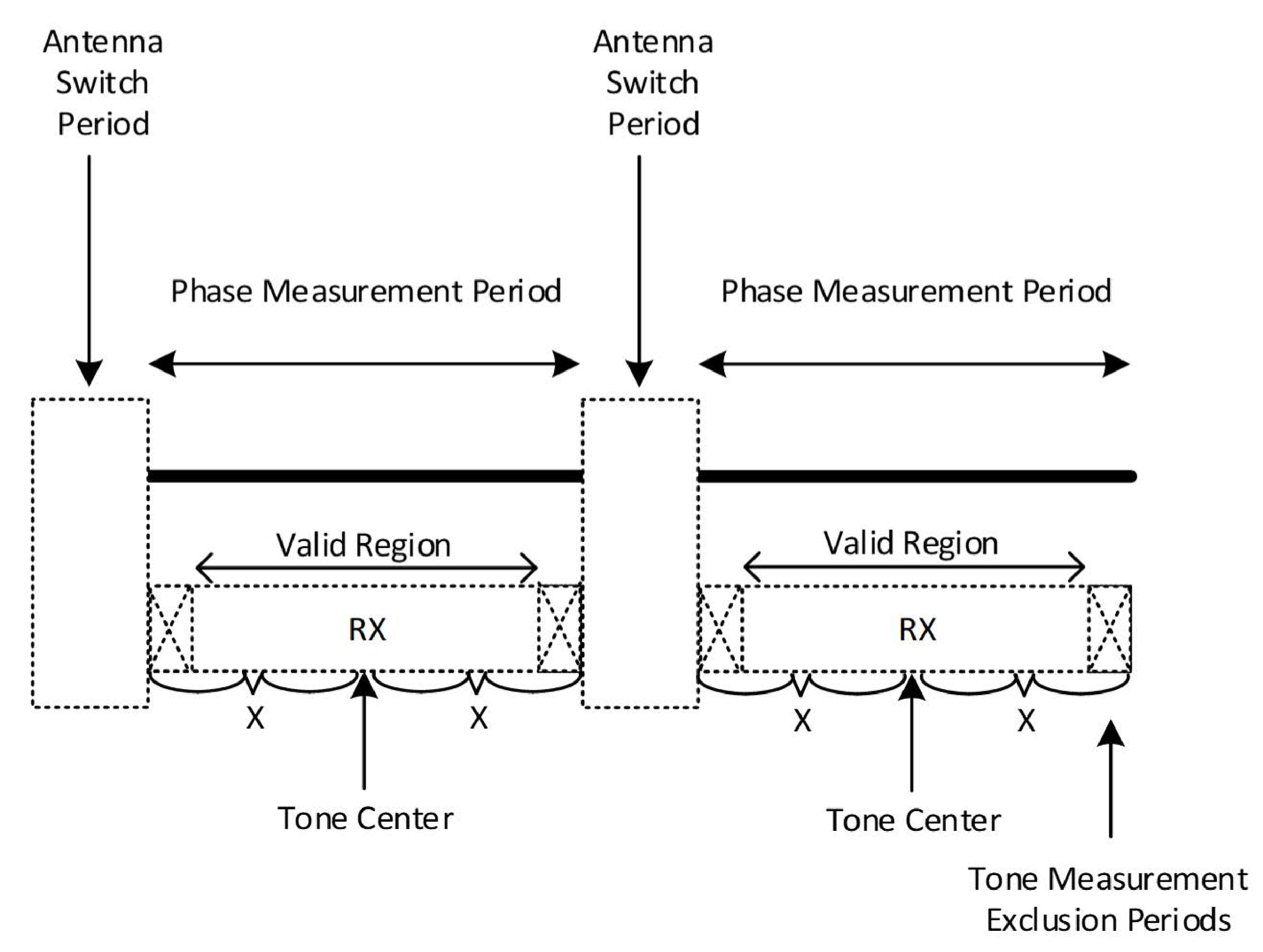
The PCT value is measured during the tone’s phase measurement period of length T_PM as shown in Figure 6.1. If there is no antenna switching, the phase measurement period of the tone represents the entire tone. If the measurement involves antenna switching, then the phase measurement period of the tone represents the time between antenna switch periods. In addition, a 1 µs tone measurement exclusion period is defined for the receiver (see [Vol 6] Part H, Section 4.6) to compensate for device clock drift, which might introduce some ambiguity as to the precise location of the beginning and end of the phase measurement period. The valid region of the tone is the time between the exclusion periods.
A frequency actuation error will cause the phase of this tone to increase or decrease linearly during a tone. The PCT term should represent the phase measured in the center of the valid region of the tone so that the corrected PCT term described in Section 6.3 can be used to compensate for the local frequency actuation error (LFAE). A device should not compensate for any residual frequency error it observes during the phase measurement period except its own LFAE.
 |
In addition to the phase, the amplitude of the PCT is used to convey the measured signal amplitude as described in [Vol 6] Part H, Section 4.6. Any frequency offset caused by a frequency actuation error should not impact the measured amplitude.
Appendix A. Test Conditions
A.1. Normal operating conditions
A.1.1. Normal temperature and air humidity
The normal operating temperature shall be declared by the product manufacturer. The nominal test temperature shall be within ±10°C of the normal operating temperature.
A.1.2. Nominal supply voltage
The nominal test voltage for the equipment under normal test conditions shall be the nominal supply voltage as declared by the product manufacturer.
Appendix B. Example test equipment setup for Channel Sounding receiver and transmitter
Figure B.1 shows a block diagram of components used to verify CS phase-based and round-trip time reporting accuracy. The vector signal generator represents the reference transmitter and transmits CS tones and packets toward the IUT (Implementation Under Test). The IUT transmits CS tones and packets toward the reference receiver represented by the vector signal analyzer. The vector signal generator and the vector signal analyzer are synchronized with the timing cadence of the CS procedure as described in [Vol 6] Part H, Section 4.5. In Figure B.1, x(t) represents the capture by the vector signal analyzer of the RF signal for each CS step. This capture should be continuous and should include the TX packet from the vector signal generator and the TX packet from the IUT.
